A p-type semiconductor is formed by introducing trivalent elements, such as boron, into pure silicon. These atoms have three outer electrons and create incomplete bonds with silicon atoms, leading to the creation of holes—locations where electrons are absent. The passage of electric current is made possible by these holes, which serve as positive carriers. Despite the doping, the material remains electrically neutral, since the number of positive charges (protons) matches the number of negative charges (electrons). An n-type semiconductor, on the other hand, is made by adding pentavalent elements like antimony, which possess five valence electrons. The crystal’s conductivity increases as the extra electron from these atoms becomes free to move easily through it. Like the p-type, the n-type semiconductor is also electrically balanced, maintaining equal total positive and negative charges. A pn junction forms when p-type and n-type regions are combined in the same silicon crystal, serving as the basic structure of a semiconductor diode. In this junction, holes act as the primary charge carriers on the p-type side, while free electrons are the main carriers on the n-type side. These two types of carriers dominate their respective sides at the junction. Both sides also have a small number of minority carriers generated by thermal energy—electrons in the p-region and holes in the n-region.
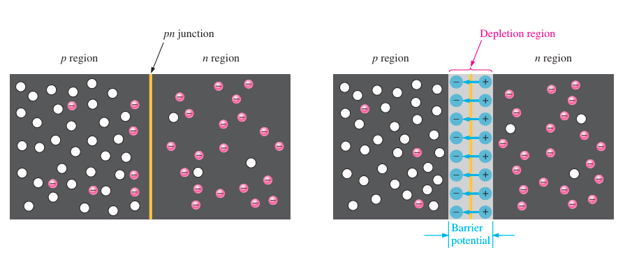
How the depletion region forms?
Electrons in the n-type region are in constant, random motion. When a pn junction is established, some electrons naturally move into the p-region and recombine with available holes. This process reduces the number of mobile charge carriers near the boundary. As electrons leave the n-side, they leave behind immobile positive ions (from donor atoms), while the recombination in the p-region leaves behind negatively charged ions (from acceptor atoms). These fixed ions create a narrow zone around the junction that is free of movable charge carriers—this is the depletion region, so named because it is depleted of free electrons and holes. The number of fixed charges increases as more carriers diffuse across the junction and recombine, resulting in the formation of an electric field. The electric field continues to grow in intensity until it is capable of blocking further electron movement across the junction. When the repelling force of this electric field balances the diffusion force, the system reaches equilibrium. At this point, the depletion layer acts as an electric barrier, halting the natural flow of charges without any external voltage. Recognizing the Potential Obstacle When positive and negative charges are separated, they generate an electrostatic force, as explained by Coulomb’s Law. An electric field that prevents further electron movement from the n-type side to the p-type side is created in the depletion zone by the fixed charges on either side. To overcome this field and push electrons through the barrier, external energy is required. The smallest amount of voltage required to overcome this barrier is known as the barrier potential.
In order for charge carriers to cross the junction and conduct current, this potential difference needs to be applied in the right polarity and magnitude. The barrier potential varies depending on factors such as the semiconductor material used, the level of doping, and the surrounding temperature. At room temperature (25°C), silicon generally has a barrier potential of about 0.7 volts, whereas germanium has a value close to 0.3 volts. Due to its common use in electronic technology, silicon is the most frequently utilized material in practical applications.
Energy Bands in a PN Junction:
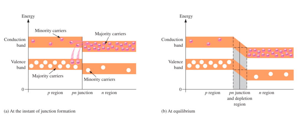
In an n-type semiconductor, the energy levels of the valence and conduction bands are slightly lower compared to those in a p-type semiconductor. This difference arises because p-type materials are doped with trivalent elements, while n-type materials are doped with pentavalent elements. Trivalent atoms exert weaker attractive forces on their outer electrons than pentavalent atoms. As a result, electrons in p-type materials tend to occupy slightly larger orbits, which means they possess higher energy than electrons in n-type materials.
At the moment the pn junction is formed, this energy difference is reflected in the energy band diagram. The conduction and valence bands on the n-side sit lower than those on the p-side, although there is some overlap between the bands. High-energy electrons in the n-type conduction band can move easily across the junction without needing additional energy. Once they enter the p-type region, they settle into the lower energy levels of the p-type conduction band. These electrons then lose energy and fall into holes in the valence band of the p-side.
As more electrons diffuse from the n-region to the p-region, a depletion region begins to form. The departure of high-energy electrons causes a drop in the conduction band energy level on the n-side. This shift is due to the gradual loss of energetic electrons that have crossed into the p-type side. Eventually, no electrons in the n-region’s conduction band have enough energy to continue crossing into the p-region. At this point, the highest energy level of the n-region conduction band lines up with the lowest energy level of the p-region conduction band, indicating that the system has reached equilibrium.
The formation of the depletion region results in an energy gradient across the junction—often described as an “energy hill” that electrons must climb to move from the n-region to the p-region. As the conduction band in the n-region moves downward, the valence band shifts downward as well, maintaining the same energy gap between the conduction and valence bands. This indicates that although the overall energy levels are altered, the amount of energy needed to move an electron from the valence band to the conduction band stays the same.