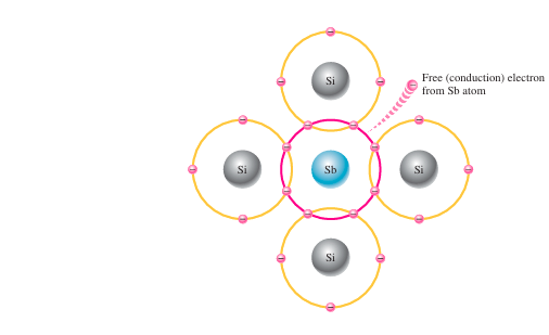
N-type semiconductor:
To boost the number of conduction-band electrons in pure silicon, elements with five valence electrons—like phosphorus (P), arsenic (As), antimony (Sb), and bismuth (Bi)—are added as impurities. Pentavalent elements, when introduced into silicon, supply additional electrons to its atomic structure, which increases its electrical conductivity. As an example, when antimony, which has five valence electrons, is introduced into silicon, it forms covalent bonds with four neighboring silicon atoms. Four of its electrons participate in bonding, while the fifth electron remains free and does not form a bond. This lone electron becomes a free conduction electron, which enhances the electrical conductivity of the silicon.
This free electron enhances the electrical conductivity of the silicon. Pentavalent elements are known as donor atoms since they provide extra electrons that enter the conduction band. The amount of conduction electrons introduced into the silicon can be precisely managed by controlling the quantity of these donor impurities. Importantly, because the additional electron is not required for bond formation, it does not create a hole in the valence band—making it an excess charge carrier added directly to the conduction band.
Majority and Minority carriers:
Since most of the current carries are electrons, silicon (or germanium) doped with pentavalent atoms is an n-type semiconductor (the n stand for the negative charge on an electron).The electrons are called the majority carries in n-type material.
Minority carriers:
Although the majority of current carries in n-type materials are electrons, there are also a few holes that a created when electron-hole pairs are thermally generated. Adding pentavalent impurity atoms does not lead to the formation of holes. In n-type materials, the few holes that do exist are referred to as minority carriers.
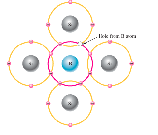
P-type semiconductor:
Since most of the current carries are holes. When silicon or germanium is doped with trivalent elements, it forms what is known as a p-type semiconductor.
To raise the number of holes in pure silicon, trivalent impurity elements are introduced into the material. These are atoms with three valence electrons such as boron (B), indium (In), and gallium (Ga). A trivalent atom like boron forms covalent bonds with four surrounding silicon atoms when introduced into the silicon lattice. Since boron has only three valence electrons, all of them are used in bonding, but one bond remains incomplete due to the lack of a fourth electron, creating a hole. These holes occur because the atom can accept an electron, which is why trivalent atoms are called acceptor atoms. The quantity of holes produced can be accurately regulated by varying the concentration of trivalent impurity atoms introduced into the silicon. Importantly, this type of doping creates holes without producing any free conduction electrons.
Majority and minority carriers:
“Holes act as the main carriers of electric charge in a p-type semiconductor.” While holes are primarily responsible for electrical conduction, a small number of electrons in the conduction band are also present due to the thermal generation of electron-hole pairs. “The electrons present in the conduction band do not originate from the addition of trivalent impurities.” Instead, they occur naturally and are considered minority carriers in p-type semiconductors.