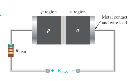
A diode functions by applying a direct current (DC) voltage across its terminals. When the diode is forward-biased, it permits current to flow through the p-n junction. This is achieved by connecting a DC voltage source across the diode using conductive elements such as wires and resistors, in a direction that establishes forward bias.
To prevent the diode from being damaged by excessive current, a resistor is used in the circuit to limit the forward current to a safe value. Forward biasing a diode involves connecting the negative terminal of the power source to the n-type region and the positive terminal to the p-type region. Additionally, the applied voltage must exceed the diode’s built-in potential barrier.
Under forward bias, the negative terminal of the voltage source drives the free electrons in the n-type region toward the p-n junction, as like charges repel each other. This movement of electrons is known as electron current. The power source steadily supplies electrons to the n-type side through the external path, enabling an uninterrupted flow of current.
The applied bias voltage gives free electrons enough energy to cross the depletion barrier and enter the p-type region. Once they arrive in the p region, these electrons have lost so much energy overcoming the barrier that they quickly fall into the valence band by recombining with available holes. At this point, the electrons are now part of the valence band within the p region due to their energy loss during the transition.
Because opposite charges attract, the positive terminal of the bias source pulls these valence electrons toward the left end of the p region. The holes—being the majority charge carriers in the p-type material—act as the path that allows valence electrons to move across the region. As electrons jump from one hole to the next, they effectively flow toward the left, while the holes themselves seem to drift toward the junction on the right. Although the holes aren’t physically moving, their effective motion creates what is known as “hole current.” Essentially, this current can also be understood as the flow of valence electrons through the p-type region, with the holes facilitating their passage.
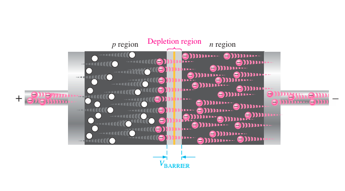
As electrons exit the p region via the external conductor and move toward the positive terminal of the bias voltage source, they leave behind holes in the p-type material. In metallic conductors, the conduction and valence bands overlap, enabling electrons to move easily with far less energy than what is required in semiconductors. Also, metals do not contain holes in their structure. Meanwhile, a steady supply of holes appears to move toward the pn junction, where they continuously recombine with incoming electrons crossing into the p region.
The Effect of Forward Bias on the Depletion Region:
When more electrons enter the depletion region, the amount of positive ions present is lowered. Similarly, as more holes effectively move into the depletion region from the other side of the pn junction, the number of negative ions is also reduced. These reduction in positive and negative ions during forward bias causes the depletion region to narrow.
The Effect of the Barrier Potential during Forward Bias:
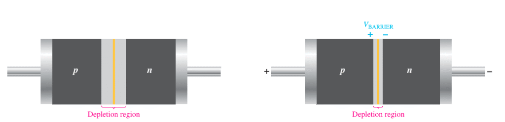
Remember, the electric field formed by the positive and negative ions on both sides of the depletion region creates an “energy barrier” that stops free electrons from crossing the junction when the system is at equilibrium. This is known as the barrier potential.
When a forward bias is applied, the bias-voltage source supplies free electrons with enough energy to surpass the barrier potential, allowing them to “climb the energy hill” and move across the depletion region. In essence, as electrons pass through the depletion zone, they lose energy equal to the barrier potential. This energy loss appears as a voltage drop across the pn junction, typically around 0.7 volts. Additionally, there is a slight voltage drop across the p and n regions caused by the internal resistance of the semiconductor material. For doped semi conductive material, this resistance, called the dynamic resistance, is very small and can usually be neglected.